Homework 7A
Demos!
An in-person demo will be required for full credit. Pay careful attention to the details below to prepare for the in-person demo!
The demo must be completed within 10 days of the due date.
What’s due & why
- Updated RISC-V design that implements additional instructions and any corresponding updates to your work from Homework 6B and 6A. As with prior assignments, your completed code needs to be submitted (via GitHub) to Gradescope. A significant portion of the grade comes from passing unit tests. (Unit tests will only include the hardware updates, not changes to the code. The code will be a part of the demo)
- Questions: The GitHub submission needs to include completed answer to the questions in
questions.mdin the repo. - An in-person demo (during office hours) is required for full credit.
Why
The goals of this assignment are to summarize and combine multiple aspects of the course:
- Continue to explore the design of computers by taking a deep look at the control and data path for a RISC-V single-cycle microarchitecture.
- Review details of program execution and performance (i.e., identifying how to delay for a given time and a large program from smaller parts via reusable functions)
- Ensure everyone has another opportunity to take a digital design and generate real-world hardware that implements that design.
(All are overall learning outcomes for the course)
Overview & Context
Now that SH Enterprises has developed a RISC-V controller for their Wonder Washer line (Homeworks 6A & 6B), they’ve run into a bit of a common engineering dilemma: Their supply chain has been disrupted by world events. In particular, the RISC-V processors they were planning to use have limited availability and are substantially more expensive than they were when the were doing R&D on the new design. This means they won’t be able to build enough Wonder Washers (their main problem) and the ones they can build will be a bit more expensive (lesser concern).
Fortunately they acquired a huge inventory of FPGAs for the original model of the Wonder Washer (i.e., Homework 4B). They considered re-designing the RISC-V Washer implementation (from Homeworks 6A and 6B) to use a HDL….but then the co-CEOs had an insight: The RISC-V processors are more expensive for everyone and SH Enterprises has a huge inventory of unused FPGAs! There may be some advantage to turning their existing inventory of FPGAs into RISC-V processors for both their needs and to potentially sell to others.
SH has tasked you to become their Director of Washing and Computing (also known as the “Director of Cleaning Computing”). They ask that you update a HDL implementation of a RISC-V processor to support instructions needed for the Washer code (from 6A and 6B) that you’ve already written. (They’re calling it “Project RISCy”) If that effort is successful, they’ll consider further updates that would allow the FPGAs to become full featured RISC-V processors, and then they can take advantage of the current market demand for RISC-V processors. (Your role is just this initial proof-of-concept processor that’s focused on the Washer from 6A & 6B)
Part 0: Setup
Link to get the repository / codespace: link
Background
RISC-V Model
SH’s co-CEOs have found an incomplete Verilog RISC-V Model. It’s a single-cycle CPU and includes a full data path and the elements that control the datapath. It supports only the following instructions: lw, sw, add, sub, and, or, xor, sll, srl, slt, addi, andi, ori, xori, slli, srli, slti, beq, bne, and jal.
The model also uses a Harvard Architecture. One of the side-effects of the way it is currently implemented is that it will not support initializing anything in the .data segment.
Hardware Interface
Homework 6B used ecalls to interact with hardware. Other engineers had already written the “operating system” components. SH has had to re-engineer that work to make it compatible with the really simple RISC-V model. They have chosen to use memory mapping. The CPU will interact with hardware as though it’s memory. Memory location 0x8000 will be used for reading and writing to the right-most 7 segments. A sw would be used rather than an ecall with a0 set to 0x152. A memory location exists to support each of the ecalls from 0x150-0x156:
| Ecall | Use/Meaning | Memory Mapped approach |
|---|---|---|
0x150 |
Set LEDs |
sw to 0x8008
|
0x151 |
Get LEDs |
lw to 0x8008
|
0x152 |
Set right 4, 7-segment displays |
sw to 0x8000
|
0x153 |
Get right 4, 7-segment displays |
lw to 0x8000
|
0x154 |
Set left 4, 7-segment displays |
sw to 0x8004
|
0x155 |
Get left 4, 7-segment displays |
lw to 0x8004
|
0x156 |
Get buttons |
lw to 0x800C
|
Their programmers have already written code that can mimic the behavior of the ecall, which looks like:
.text
.globl ecall_proxy
ecall_proxy:
  ...

  li s0, 0x8000     # Use s0 to refer to 0x8000.  Use offsets from here

  ...

ecall_proxy_right_7segs:
  li s1, 0x152
  bne a0,s1, ecall_proxy_left_7segs
  sw a1, 0(s0)      # Storing the segment values to 0x8000
  j ecall_proxy_end

  ...
You can use Task 4.4: Edit common_ice40.S to see the entirety of this function.
There are three important things to note here:
- You’ll need to replace
ecallwithcall ecall_proxyin prior code. -
callis a pseudo-instruction that can turn into either ajalor a combination of both a `auipc` and a `jalr`.- The you’ll need to
calltheecall_proxy. The processor will need to be able to support all three “real” instructions to be able to safely handle doing acall ecall_proxy.
- The you’ll need to
- The
liis also a pseudo-instruction. It can turn into either anaddior a combination of both an `lui` and anaddi.- The
ecall_proxydoes anli 0x8000. This translates into the form that useslui. Again, you’ll need to support both “real” instructions that may be used for thelipsuedo-instruction.
- The
- The
jr(andret) are also pseud-instructions. Both become ajalr.- We need
jalrto support any form of functions.
- We need
Part 1: Adding Instructions
Caution!
This is a real-world example of a significant computer engineering task. You need to have a plan rather than just opening the Verilog file and typing.
The risc-v folder contains a Verilog implementation of a partial RISC-V processor (an implementation that corresponds to our textbook). The Edit riscvsingle.sv task can be used to open it.
It is a single-cycle CPU and includes a full data path and the elements that control the datapath. It supports only the following instructions: lw, sw, add, sub, and, or, xor, sll, srl, slt, addi, andi, ori, xori, slli, srli, slti, beq, bne, and jal.
An analysis of the code needed for the Wonder washer highlighted three significant omissions:
- It doesn’t support
lui, which is needed for the implementation ofecall_proxythat will be used to control the washer’s outputs. - It doesn’t support either of the instructions needed for one of the forms the
callmay translate to: it doesn’t support eitherjalrorauipc.
Part 1.1: Process and lui
- Start with:
- a diagram of the single-cycle CPU:
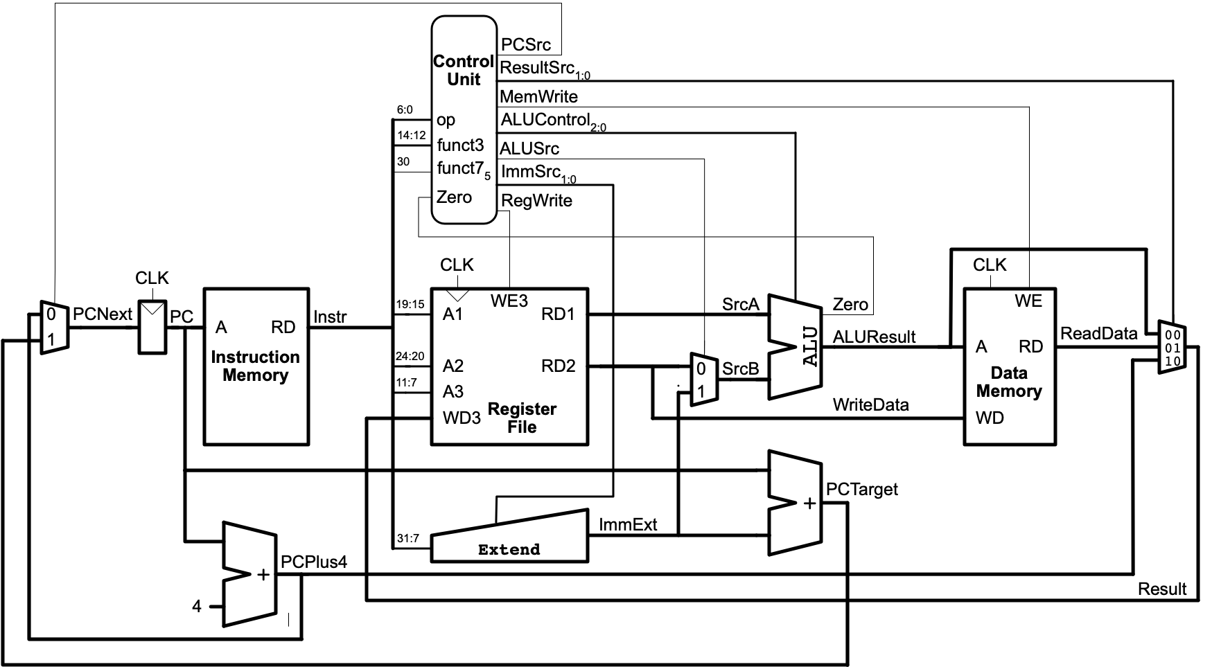
(Figure 7.15 from Digital Design and Computer Architecture, RISC-V Edition by Harris & Harris)
-
Review
lui, its meaning/behavior (also referred to as its “semantics”), and its format in Figure B.1 and Table B.1. In particular the last column (Operation) gives a precise description of how the instruction impacts the machine state. -
You’ll also need to understand how various parts of this CPU implementation that aren’t fully described in the diagram behave. The parts that aren’t shown in the diagram are the ALU (Table 7.3, page 409) and the Extend unit (Table 7.5, page 412).
-
Develop a plan for how the existing design can be modified to support
luiand annotate it on the diagram. It may help to re-read/review 7.3 of the text.Caution!
If you come to office hours or need help on this part, the first question will be “show us your diagram”. We will need to know what you want to do before we can help.
-
Code review: The HDL model in
riscvsingle.svrepresents a significant part of a RISC-V CPU. It contains a hierarchy of multiple modules. At the top of that hierarchy is theriscvsinglemodule. It contains the two major aspects of a simple CPU: acontroller, which decodes instructions, and configures the other element, thedatapath. As the name implies, thedatapathencompasses all the components that process data.- Review the various modules in
riscvsingle.svand update your diagram with details about which modules correspond to which parts of the diagram. For example, there are actually two Verilog modules that correspond to the Control Unit. Also, look carefully for the types of signals that are important for your approach to supportinglui.
- Review the various modules in
- Identify a plan to update
riscvsingle.svto supportlui(there are multiple valid approaches). Updateriscvsingleand check your work with the provided testbenches.-
RISC-V lui Testbench(risc-v-lui-tb.sv): This tests a few variations ofluiinstructions and confirms that machine state is altered in expected ways. It also includes some checks to confirm it’s not altered in unexpected ways. This will help test that yourluiworks without consideration for other instructions. If successful, thePROBLEMSpanel will show an entry forrisc-v-lui-tb.svthat says “All tests passed!”. If not successful, it will contain some details about the specific instruction that failed. As usual, you can use the waveform views to try to better understand errors.
-
Part 1.2: jalr
Repeat the steps/process described above to add support for the jalr instruction. You can use the RISC-V jalr Testbench (risc-v-jalr-tb) to confirm that your implementation seems to behave correctly for a few test cases.
Part 1.3: auipc
Repeat the steps/process described above to add support for the auipc instruction. You can use the RISC-V auipc Testbench (risc-v-auipc-tb) to confirm that your implementation seems to behave correctly for a few test cases.
More Testing
The prior test benches only help confirm that execution of the new instructions themselves may be ok. Often making changes can have side-effects that break things that worked before. RISC-V general Testbench (risc-v-gen-tb) tries nearly all instructions once, including the lui, jalr, and auipc. It isn’t a very rigorous test, but it will help confirm that changes probably didn’t interfere with the behavior of other instructions. If successful, the PROBLEMS panel will show an entry for risc-v-gen-tb.sv that says “All (279) test passed!”.
RISC-V Program Testbench (risc-v-prog-tb) runs a full program that test many, but not all, instructions (it does not test jalr or auipc). It’s primary function is to make sure a full program using lui and all prior instructions appears to still work (mostly a Regression Test). ` If successful, it will show Simulation succeeded! in the Problems tab.
Debugging the Data Path
The waveform view allows you to see the step-by-step execution of a program and look at all components of device under test (that is, the CPU). Here’s an example of using waveforms to understand what’s going on:
Do-overs
You may find that you want to Revert your changes if things aren’t working out. You can easily retrieve the original code via git or GitHub. Here are two approaches:
- Go to the repository on GitHub.com, click on the file of interest, then click on the
Historybutton, and finally select a specific version to view (if you haven’t pushed updates to GitHub, only the original version will be shown). You can copy/paste the code as needed. - Right-click on a file in the CodeSpace file explorer and select
Open Timeline. ATIMELINEview will be shown in the explorer panes and you can select an older version of the work, which will be compared with the current version. The timeline includes bothgitcommits and the times the file has been saved since you opened the Codespace session.
Part 2: Code
Caution!
Our processor is small, and limited. You may have to adjust your code to conform to the limitations:
- It only supports
lw,sw,add,sub,and,or,xor,sll,srl,slt,addi,andi,ori,xori,slli,srli,slti,beq,bne,jal, and (now)lui,jalr, andauipc. Check that the generated ROM only contains these instructions.- Pseudo-instructions that are converted to the supported instructions can be used in your source assembly language. For example,
liis ususally converted to a combination ofaddiand/orlui,callis often converted tojalorjalrandauipc, etc.
- Pseudo-instructions that are converted to the supported instructions can be used in your source assembly language. For example,
- It does not support using
.data(for global variables) at all. - It is limited to 2047 words of RAM.
- The ROM is limited to about 500 words (500 instructions!)
Part 2.1: delay() (with more accuracy)
The delay.S (Edit delay.S) is mostly empty. You should start by copying your delay() code from prior assignments. Make sure it’s set up for the simulated environment initially. The Simulate delay.S task will loop through showing the numbers 1, calling delay(1000), 2, calling delay(2000), and 5, calling delay(5000). Test it out in the simulator.
We now have a single-cycle processor that operates on a clock cycle of 6 MHz. That is much, much faster than the simulator and will be very consistent. You can come up with a precise formula for how many instructions would execute in a given time. Comment out the computation needed for simulation and update your code to work with this new microarchitecture. You are limited on the instructions you can use (no div or mul). Ensure delay() will be within about 10% accuracy (you can assume it’ll only be used on values >100ms). Be sure to heed the warnings above about available instructions!
Once you feel that your code is correct, you can convert it to a “ROM” suitable for your hardware via the Convert delay.S+driver for iCE40 ROM task. The resulting file includes both some driving code (first) and your delay()’s code. Review the details of the ROM to confirm that it meets the above requirements! (That is, not using unsupported instructions, not using anything in .data, and not too long)
Finally, you can use the RISC-V+delay.S bitstream to create a file to program your FPGA. This design is more complex than prior designs, so this process will take longer!
Part 2.2: Re-spinner()ing
Edit spinner.S can be used to edit a empty version of the spinner() function. As before, paste in your code from prior assignments.
You will need to replace any ecall with a call ecall_proxy. Since this is now a function call, you will also need to ensure your code follows the register use conventions!
You can simulate it via the Simulate spinner.S task, but be sure to change your delay() to use values that are appropriate for the simulator. The simulated version of the spinner will iterate through four examples: spinner(1,500,0), spinner(2, 250, 1), spinner(3, 125, 2), and spinner(4,62,3).
You can use the Convert spinner.S+driver for iCE40 ROM task to convert it to machine code. As before, make sure your code meets the requirements. Once done, you can use the RISC-V+spinner bitstream task to convert it for programming the FPGA.
Part 2.3: Wonder Washout
Once the prior two parts work on the hardware, it’s time to try the complete washer state machine! Again, use Edit washer.S to add your prior work and review the requirements, making any updates that may be needed.
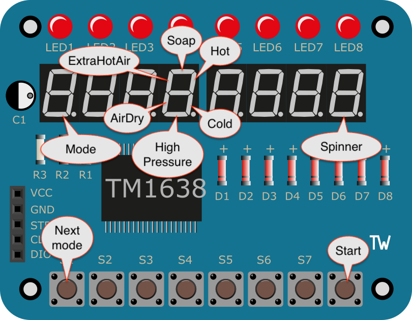
Again, after ensuring delay.S is configured for simulation, you can use Simulate washer.S to simulate the behavior. Once you know it works, updated delay.S to be appropriate for the hardware and use Convert washer.S+driver for iCE40 ROM, then check the resulting assembly language. Finally, the RISC-V+washer.S bitstream can be used to prepare it for the FPGA. It will use hardware as in Homework 6B:
And a demo:
Part 3: questions.md
As in past assignments, complete the questions in questions.md.
Submission
As with Homework 6A, you will need to commit and push work to GitHub and then go to Gradescope to “pull” the work over.
For full credit you also need to do an in-person demo during Office hours. You should bring any diagrams/notes about how you modified the CPU to support lui, jalr, and auipc and be prepared to discuss your work, including the assembly language code.
- Submission Link: Gradescope